AI-Powered Metrology Boosts Semiconductor Yields
Semiconductor manufacturing requires levels of reliability that would be outlandish to expect in other contexts. For example, the quality of a semiconductor component is usually measured in defects per million (DPM).
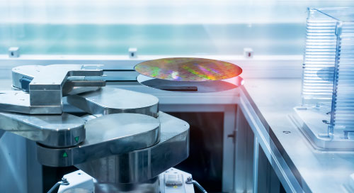
To achieve these measurements, semiconductor metrology uses optical tools and an electron beam to scan wafers for defects early in the manufacturing process—preventing the use of bad wafers and the resulting nonfunctional chips.
But as semiconductors are manufactured on increasingly smaller process nodes, it has become more difficult to accurately detect wafer defects with traditional metrology. Where metrology equipment alone is no longer capable of detecting defects as quickly or accurately as semiconductor engineers would like, artificial intelligence (AI) is now being used.
A Closer Look with AI
Today AI is being integrated into wafer inspection, defect detection and classification, and scanning electron microscope (SEM) denoising. This enables making advanced correlations between metrology readings and data from manufacturing sensors.
Adding AI testing to the semiconductor manufacturing process helps engineers find hidden signals from all of these inputs. But this requires new equipment to execute demanding computer vision and other deep neural networks at the edge. And the high-performance processors needed to run these AI workloads must be cooled without disrupting the highly sensitive environmental requirements of fabrication facilities.
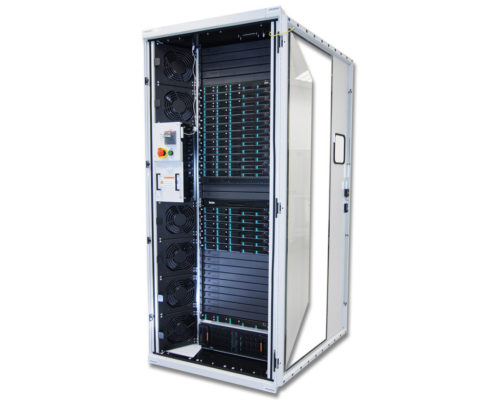
Prodrive Technologies, an embedded systems and solutions provider, addresses this challenge with its Zeus High-Performance Cabinet (ZHPC). The system is designed to hold high-performance servers capable of transforming metrology signals into actionable intelligence (Figure 1).
To support metrology operations, it uses an internal, liquid-cooled heat exchanger to dissipate thermal energy without exhausting dirty air into its surroundings or venting from the outside. This allows it to be deployed in the sub-fab, below a foundry’s clean room, where there are strict air control standards.
The Zeus High Performance Cabinet provides coolant leakage and smoke detection, and can house, power, and cool as many as 41 rack servers. @prodrivetech via @insightdottech
The Zeus High Performance Cabinet provides coolant leakage and smoke detection, and can house, power, and cool as many as 41 rack servers. This includes high-performance servers such as the Zeus Scalable Series of high-density server platforms based on 3rd generation Intel® Xeon® Scalable processors, previously called Ice Lake.
High-Performance Compute for AI-Enabled Metrology
The latest Intel Xeon devices are built on a 10 nm process and integrate technologies such as Intel® Advanced Vector Instructions 512 (Intel® AVX-512) and Intel® Deep Learning Boost (Intel® DL Boost). These help the Zeus servers run advanced neural networks that chew through metrology data efficiently.
Intel AVX-512 is a set of instructions that supports enhanced vector processing, including the ability to execute 32- or 64-bit single-precision, floating-point operations per clock cycle. Along with two fused multiply-add (FMA), these instructions allow the Xeon devices to perform complex math operations required for AI algorithm computation.
Intel DL Boost technology builds on those features of AVX-512 to include Vector Neural Network Instructions (VNNI) and support for bfloat16 math operations, which are even more efficient in AI workloads than the single-precision, floating-point math mentioned previously. As a result, platforms based on the 3rd gen Xeon are able to double the performance of certain deep-learning tasks.
Beyond computing performance, the processor supports PCI Express Gen 4.0 and its 64 Gbps of bandwidth. This means that the Zeus portfolio can be deployed near optical and e-beam inspection tools in the sub-fab, without being overwhelmed by the massive amounts of data they produce. By eliminating any bottlenecks in local bandwidth, all metrology data and analysis can be performed at the edge to reduce latency and security concerns associated with transmitting to external systems.
Without limitations of bandwidth or processing power, the Zeus HPC and scalable servers can function as an all-in-one networking, CPU, and storage platform that integrates AI into wafer testing tools. This in turn speeds the inspection process and improves final semiconductor yields.
“The way we see it is that you can have a cloud and edge architecture inside the fab, and now everything is done at the tool,” says Bas van Bree, program manager with Prodrive Technologies. “By centralizing workloads, we can get an optimization of the amount of compute resources that are available inside a fab.”
There’s broad agreement in the industry that AI and ML are vital to hitting acceptable yields as CPU feature sizes continue to shrink and demand for improved performance and efficiency increases. But it requires processing platforms with enough performance, the right technology, and the ability to be deployed at the edge where it can conduct analysis in real time.