Balanced Approach Gives Semiconductor Equipment New Life
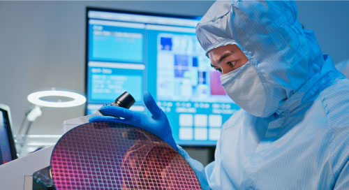
Semiconductor manufacturing equipment is some of the most expensive in the world, with the average price of each piece of machinery easily exceeding $1 million. Certain instruments, like extreme ultraviolet (EUV) scanners, can potentially cost hundreds of millions.
As you can imagine, semiconductor manufacturers want to protect these investments. And if the initial price tags weren’t enough of a reason, secondary markets have formed around these commodities to extend their operational life for decades after initial deployment.
Obviously, these two factors incentivize semiconductor equipment owners and manufacturers to keeping this machinery running optimally for as long as possible.
This desire has created an interesting dynamic in the electronics industry, where some of the most advanced technology in the world is produced using equipment that’s many generations old. Of course, these systems can be upgraded just like any other electronic system. But as they age, retrofitting semiconductor manufacturing equipment to keep pace with today’s performance standards becomes a larger and larger task.
For example, adding state-of-the-art electron beam or EUV instrumentation to a decades-old lithography machine enables fabrication of chips with miniature silicon transistors. But it also requires a massive increase in system throughput to support passing large amounts of data between the equipment’s control units on tight, deterministic schedules.
Moving Semiconductor Manufacturing from Last Gen to Next Gen
To offset the cost of perpetual upgrades, semiconductor equipment manufacturers have designed control systems around industry standards like VME for many years. First developed in the early 1980s and available from multiple vendors, the VME standard defines a consistent PCB, connector, and signaling system that allows existing boards to be substituted for new ones when damage occurs, or upgrades are required.
“You must balance 30-year-old VME #technology with the newest #CPU technology. This is the tricky thing our team is doing. Basically, they’re putting brains of super geniuses in the bodies of dinosaurs.” – Luca Varisco, Advanet via @insightdottech
In theory, this means a legacy VME control board can be substituted for one with more performance to handle the higher bandwidth required by modern semiconductor manufacturing apparatuses. But making the most of this performance requires more than just selecting a board with an advanced processor, slotting it into the system, and calling it a day.
Acquired in 2011, Advanet is a branch of the Eurotech Group that specializes in ODM services for cutting-edge systems like semiconductor manufacturing equipment. Headquartered in Japan, it works directly with many of the world’s leading semiconductor equipment manufacturers to help integrate new processor technology, legacy hardware, and communications protocols—and some of the most sophisticated instrumentation on Earth.
“In a way, you have a two-speed machine,” explains Luca Varisco, Head of Product Marketing at Advanet. “There are some parts of the machine that stay around for 30 years. At the same time, there are things that are very, very advanced and change frequently to follow the decreasing wavelengths of ultraviolet light. The shorter the wavelength, the more control you need of the machine that focuses the ultraviolet beam.
“Because of that, the CPU must also advance,” he continues. “So you must balance 30-year-old VME technology with the newest CPU technology. This is the tricky thing our team is doing. Basically, they’re putting brains of super geniuses in the bodies of dinosaurs.”
A big part of that balancing act involves the I/O subsystem, which must remain rigidly deterministic but evolve with the CPU to prevent data bottlenecks from forming between low-speed interfaces and high-performance processors. But at the same time, the entire control mechanism must stay within the power consumption and thermal dissipation envelopes of systems that predate the 2000s.
The Chips that Make the Chips
Along with operational stability and long-lifecycle support, these were key requirements in a project Advanet accepted to upgrade the control subsystem of an electron beam (e-beam) lithography machine for a leading semiconductor manufacturing equipment provider.
The primary responsibility of the particular control subsystem is to focus lenses that concentrate the lithography system’s e-beam onto a target substrate. Doing this with nm-scale precision requires extreme computational horsepower, as well as coordination of multiple control endpoints around the machine. Of course, there are countless legacy components around the machine that must interface with the control system as well.
Looking to blend the old and the new, Advanet started developing a solution around new Intel® Xeon® D-1700 processors (codenamed “Ice Lake-D”) that would eventually become the Advme8088. A 6U, 1-slot-wide VME board, the Advme8088 features Xeon D-1700 processors with up to 4 cores but TDP ratings no higher than 50 W.
Just as important, the Advanet card includes the trusted VME connector alongside modern interfaces like Serial RapidIO Gen 2, PCI Express Gen 3, and multiple Gigabit Ethernet ports.
The lithography control subsystem in question is backplane-based and consists of a VME chassis with eight to 12 Advme8088 cards, two or three custom optical boards also developed by Advanet, and a power supply. The Advme8088 and other cards plug into the backplane using VME connectors, which transmit signals between the boards and legacy components in the machine. An FPGA on the backplane itself serves as a flexible VMEbus controller that protects against obsolescence and provides some signal preprocessing.
Meanwhile, the Advanet card’s newer interfaces are what maximize the capabilities of its onboard Xeon D-1700 processor. In the lithography subsystem project, for example, Intel® Time Coordinated Computing (Intel® TCC) supported by the Xeon D-1700 and configured to work with the Advme8088’s GbE interfaces synchronizes Ethernet packets flowing between control endpoints with sub-200 µs latency.
This same control network manages the position and orientation of electron beam lenses as well as other step stages on the machine.
New Life for Legacy Lithography Equipment
Despite seemingly insatiable demand for performance, their position at the heart of many control systems will keep VME products in semiconductor manufacturing equipment for the foreseeable future.
Of course, no matter how creative your engineering team is, all technology—even those based on standards—eventually falls victim to obsolescence. You can find evidence of this in the lithography control system’s backplane FPGA, which serves, in part, as an alternative to VMEbus controller chips that are being supplied by fewer and fewer vendors while becoming more and more expensive.
For this reason, the Xeon D-1700 processor is available in extended-temperature, long-lifecycle embedded variants supported for seven years or more. For its part, Advanet commits to supporting its solutions for decades.
“It looks strange because you see VME and say, ‘30-year-old technology? What’s that?’,” Varisco explains. “But actually that’s exactly what’s missing in the semiconductor market because you can’t throw away.”
And it turns out, you wouldn’t want to. After all, when you consider the primary and secondary markets, it’s part of a multimillion-dollar machine.
This article was edited by Christina Cardoza, Associate Editorial Director for insight.tech.